Note
Go to the end to download the full example code.
Semiconductor wafer map
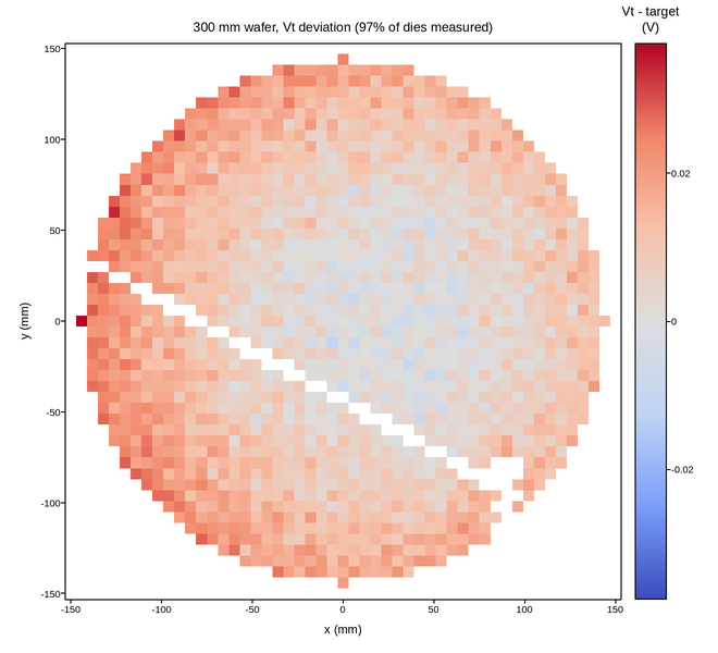
Threshold voltage measured on every die across a 300 mm wafer – the map a process engineer reads to separate a systematic process signature from random defects.
Two things make it awkward to plot. Dies outside the wafer edge do not exist,
and dies that failed electrical test have no meaningful Vt: both are nan,
so they stay unpainted and neither drags the colour range nor invents a value.
The wafer’s round boundary then appears for free, straight out of the data.
Vt is quoted against a target, and the interesting quantity is the deviation from it, which is signed. A diverging map centred on the target puts on-spec dies at the neutral midpoint, so the radial signature – here a centre-to-edge gradient from a deposition non-uniformity – reads immediately, as does the scratch across the lower right.
Live figure — pick a tool, then zoom, pan, point-pick or annotate. Nothing is active until a tool is selected.
View this figure’s Vega export ↗ — the raw JSON spec, rendered live by a real Vega engine.
View this figure’s Vega-Lite export ↗ — the raw JSON spec(s), rendered live by a real Vega-Lite engine.
import numpy as np
import polars as pl
import plotpress

rng = np.random.default_rng(41)
RADIUS = 150.0                                   # mm
TARGET = 0.450                                   # V

step = 6.0                                        # die pitch (mm)
x = np.arange(-RADIUS, RADIUS + step, step)
y = np.arange(-RADIUS, RADIUS + step, step)
X, Y = np.meshgrid(x, y)
r = np.hypot(X, Y)

# Radial deposition signature plus a slight azimuthal tilt, in volts.
vt = TARGET + 0.022 * (r / RADIUS) ** 2 - 0.008 * (X / RADIUS)
vt += rng.normal(0.0, 0.0035, vt.shape)

vt[r > RADIUS - step] = np.nan                    # off-wafer
# A handling scratch, and a cluster of parametric failures near the notch.
vt[np.abs(Y + 0.55 * X + 44.0) < 4.0] = np.nan
vt[(np.hypot(X - 92.0, Y + 96.0) < 20.0) & (rng.random(vt.shape) < 0.55)] = np.nan

# One row per die -- the shape a wafer prober's own test-log export is in,
# before it is gridded for the mesh. Off-wafer and failed dies ride along as
# nan in the value column; the x/y die-position columns stay finite.
dielog = pl.DataFrame({"x": X.ravel(), "y": Y.ravel(), "vt": vt.ravel()}).sort(["y", "x"])
x = dielog["x"].unique().sort().to_numpy()
y = dielog["y"].unique().sort().to_numpy()
vt = dielog["vt"].to_numpy().reshape(y.size, x.size)
X, Y = np.meshgrid(x, y)
r = np.hypot(X, Y)

dev = vt - TARGET
lim = float(np.nanmax(np.abs(dev)))
fig, ax = plotpress.subplots(figsize=(6.6, 6.0))
mesh = ax.pcolormesh(x, y, dev, cmap="coolwarm", vmin=-lim, vmax=lim)
fig.colorbar(mesh, ax=ax).set_title("Vt - target\n(V)")
ax.set_aspect("equal")
ax.set_xlabel("x (mm)")
ax.set_ylabel("y (mm)")
yield_pct = 100.0 * np.isfinite(vt).sum() / (r <= RADIUS - step).sum()
ax.set_title(f"300 mm wafer, Vt deviation ({yield_pct:.0f}% of dies measured)")
fig.tight_layout()
Total running time of the script: (0 minutes 0.100 seconds)